
(1) Select the correct grid -setting and always use the grid spacing that can match the most components. Although multiple grids seem to be significant, if...
Over the years, PCB seems to have been "downgraded" in the field of electronic engineering, and has become an unknown hero who silently paid behind ...
In the process of PCB design, if possible in advance to predict possible risks and avoid them in advance, the success rate of PCB design will be greatly impro...
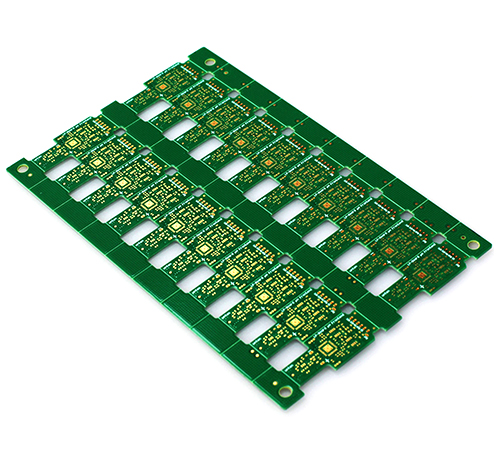
The automotive electronic market is the third largest application area of PCB after computer and communication. With the car mechanical products in the traditio...
1. From the specific circuits and functions of the board, you can choose whether the circuit on the board needs to use the corresponding test point.2. There sho...
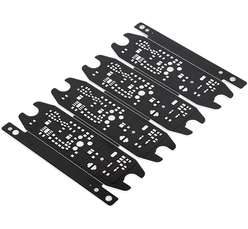
1. The process of processing equipment will be used, such as: inner front processing line, plating a copper before processing line, D/F, welding (welding) ... a...

1. The process of processing equipment will be used, such as: inner front processing line, plating a copper before processing line, D/F, welding (welding) ... a...

1. Determine the number of layers of PCB The size of the circuit board and the number of wiring layers need to be determined in the early stage of the de...

If the density of the component on the 4 -layer board is relatively large, it is better to use 6 layers. However, some overlapping schemes in the 6 -layer ...