
Service Hotline
Service Hotline


1. HASL hot air is flat (that is, tin spray often)Tin spray is a commonly used treatment method for PCB samples. It is now divided into lead spray tin and lead ...
In order to solve the above problems of the gold -plated circuit board, PCB manufacturers use the PCB of the golden board mainly to have the following character...
The layout is plain to put devices on the board. At this time, if the preparations mentioned earlier are done, you can generate a network table (design- "C...
1. Preparation includes preparation component library and schematic diagram"If you want to be good, you must first benefit your instrument." To make a...
1. High -incidence heat heating device plus radiator and heat conduction boardWhen there are a few devices in the PCB circuit board, when the heat is large (les...
When the electronic equipment works, the heat generated will increase the internal temperature of the equipment rapidly. If the heat will not be distributed in ...
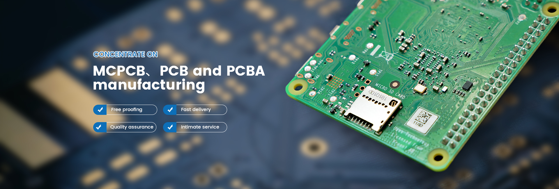
1. High reliability: We will pass a series of inspections, testing, and aging tests to ensure that the PCB circuit board will work for a long time and reliably....

So first, we need to make two layers of circuits of the middle core. After the copper clad plate is cleaned, a layer of photosensitive film will be covered on t...
The first step of PCB fabrication is to sort out and check the layout of pcb multilayer circuit board. The PCB manufacturing factory receives the CAD files from...

Offer competitive price with
superior quality

The indepent PCB and SMT
plant

Guarantee the quality and
lead time

Fastest processing in each
department
24H service hotline:
 sales@hyymcpcb.com
mkt@hyymcpcb.com
 No.10 YuMin Road, Shatou Industrial Zone, ShajingTown, Bao'an District, Shenzhen, China.


Copyright © 2013-2017 SHENZHEN HYY TECHNOLOGY CO.,LTD Technical Support: Xhyos


About Us

News

