Service Hotline

+86-0755-27266631
13923719662

News

MCPCB, PCB and PCBA manufacturing

Key words:

Single and double layers| Four-layer board| Six-layer board| Copper base/Aluminum substrate|

Home  》  News  》  Industry News

Company News

Industry News

FAQ

PCB immunity to transient conductivity and PCB immunity to electromagnetic field radiation

PCB immunity to transient conductivity and PCB immunity to electromagnetic field radiation

The ESD activity is captured by a test instrument (EUT) by discharging from the ESD simulator to the surface of the EUT and near the EUT. The severity level of ...
Detail >

Detailed analysis of vacuum etching technology in PCB production

Detailed analysis of vacuum etching technology in PCB production

The etching process is one of the basic steps in the process. To put it simply, the base copper is covered by the resist layer, and the copper that is not prote...
Detail >

Hardware structure design of numerical control device on PCB circuit board

Hardware structure design of numerical control device on PCB circuit board

The numerical control device is the core of the entire numerical control system, and its hardware structure can be divided into a large-board structure and a fu...

Detail >

What is the role of surface tension in PCBA welding and how to reduce surface tension and viscosity

What is the role of surface tension in PCBA welding and how to reduce surface tension and viscosity

The role of surface tension in welding:Surface tension is in the opposite direction to the wetting force, so surface tension is one of the factors that are detr...
Detail >

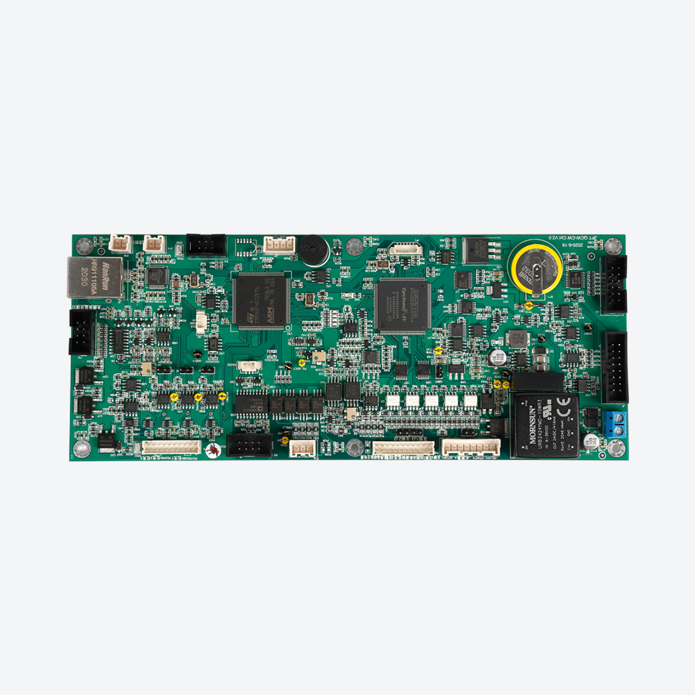
How to reduce surface tension and viscosity in PCBA soldering

How to reduce surface tension and viscosity in PCBA soldering

The main measures to reduce surface tension and viscosity in pcba welding are as follows.①Increase the temperature. Elevating the temperature can increase the m...
Detail >

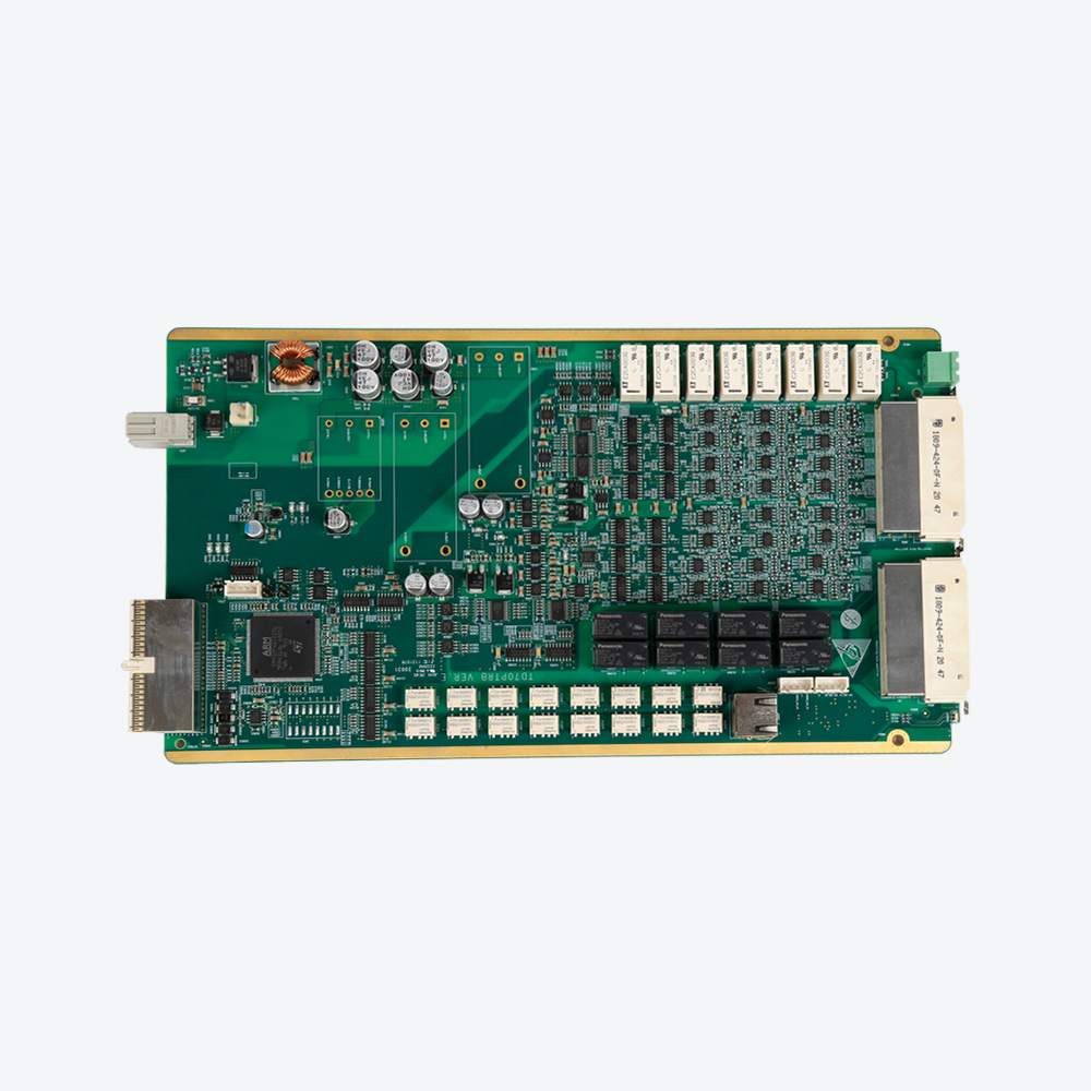
PCB Design: Additive Manufacturing Considerations

PCB Design: Additive Manufacturing Considerations

1. Definition of solder maskEssentially, the delineation provided by any EDA tool is incorrect; the CAM vector file specifies deviations from an assumed continu...
Detail >

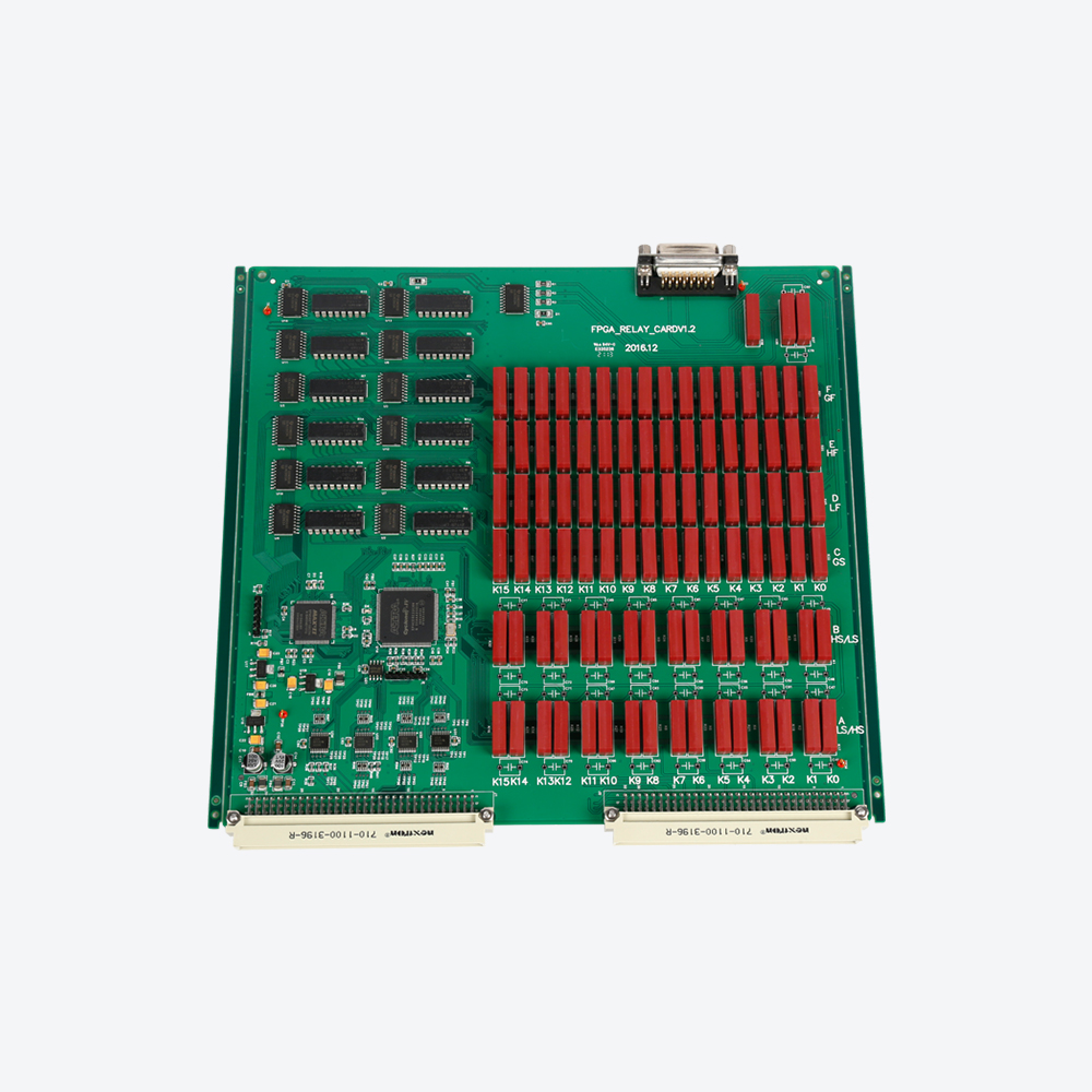
PCB special circumstances and consequences

PCB special circumstances and consequences

1) Shared clock tracesIt is better to use a radial topology connection for fast rising edge signals and clock signals than to use a single common drive source n...
Detail >

PCB Design: The Benefits of Flooring Below the Clock Crystal on a Single Board

PCB Design: The Benefits of Flooring Below the Clock Crystal on a Single Board

1. Layout1) The clock crystal and related circuits should be placed in the center of the PCB and have a good ground plane, not near the I/O interface. The clock...

Detail >

Summary of PCB Design Principles

Summary of PCB Design Principles

Principle 1: PCB clock frequency exceeds 5MHZ or signal rise time is less than 5ns, generally need to use multi-layer board design.Reason: The signal loop area ...

Detail >
  • Previous
  • 23
  • 24
  • 25
  • 26
  • 27
  • 28
  • 29
  • Next