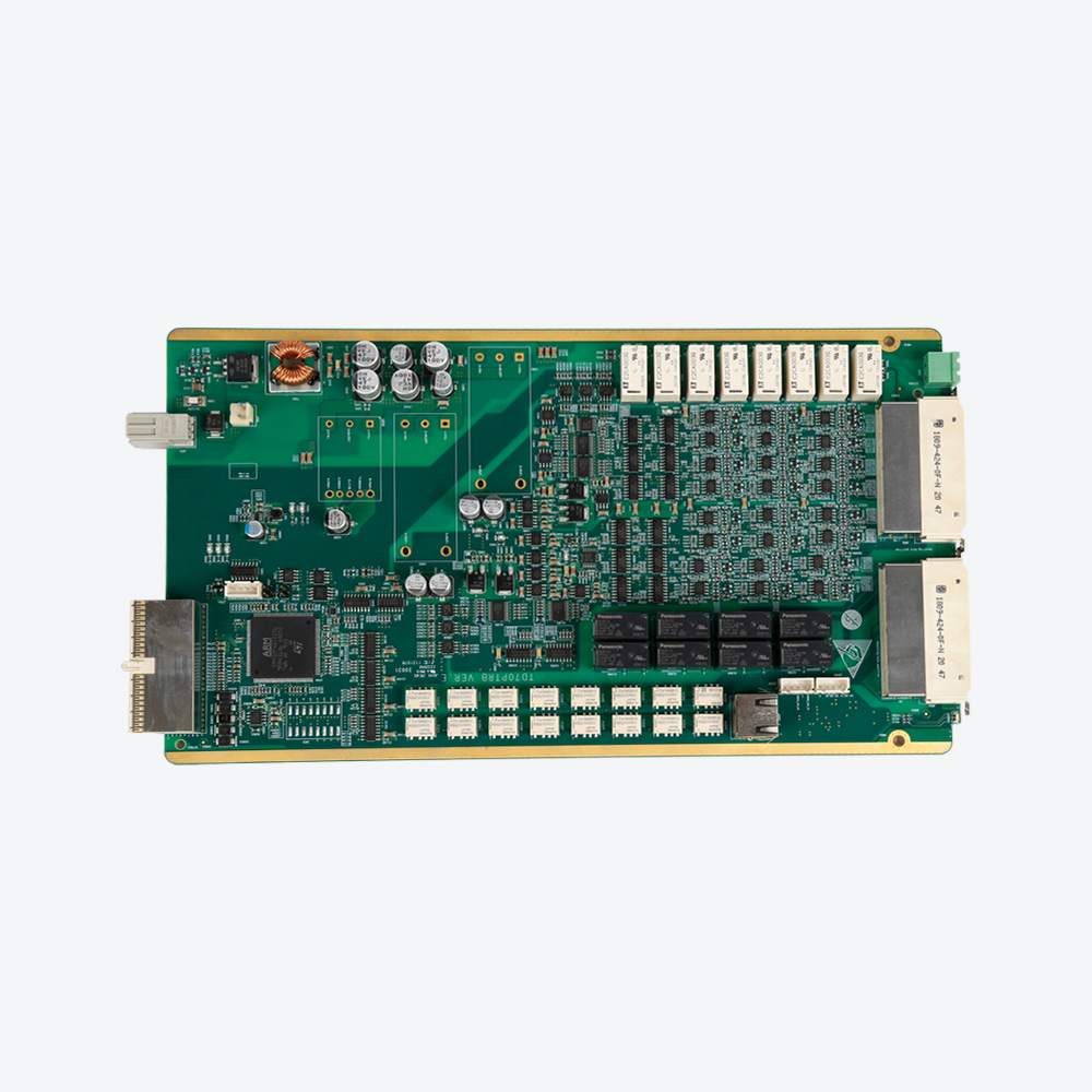
Time:2022-07-19 Visit:
1) Shared clock traces
It is better to use a radial topology connection for fast rising edge signals and clock signals than to use a single common drive source network in series. Each trace should be wired according to its characteristic impedance.
2) Clock transmission line requirements and PCB layering
pcb design
Clock routing principle: Arrange a complete image plane layer next to the clock routing layer, reduce the length of the routing and perform impedance control.
Incorrect cross-layer traces and impedance mismatches can result in:

Lines use vias and jumps resulting in incomplete image loops.
The surge voltage on the image plane due to the voltage on the signal pin of the device changing with the change of the signal.
If the wiring does not consider the 3W principle, different clock signals will cause crosstalk.
3. Wiring
1) The clock line must go on the inner layer of the multi-layer PCB board. And be sure to take the strip line; if you want to go on the outer layer, you can only take the microstrip line.
2) Walking on the inner layer can guarantee a complete image plane, it can provide a low impedance RF transmission path and generate magnetic flux to cancel the magnetic flux of their source transmission line, the closer the distance between the source and return path, the better the demagnetization . Due to the enhanced degaussing capability, each full planar image layer of a high-density PCB can provide 6-8dB of rejection.
3) Advantages of clock cloth multilayer boards: One or more layers can be dedicated to the complete power supply and ground plane, which can be designed as a good decoupling system, reducing the area of the ground loop, reducing the differential mode radiation, reducing the The EMI is reduced, the impedance level of the signal and power return paths is reduced, the consistency of the trace impedance throughout the whole process can be maintained, and the crosstalk between adjacent traces is reduced.