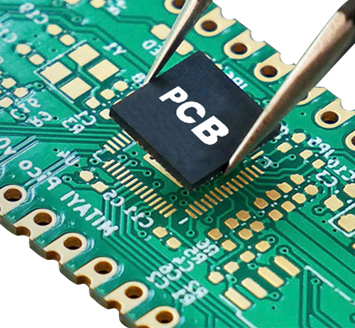
When pcb layout of circuit components, it is necessary to meet the requirements of anti-interference design1. Arrange the position of each functional circuit un...

First, consider the size of the pcb. If the pcb size is too large, the printed line will be long, the impedance will increase, the anti-noise ability will decre...
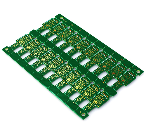
The curve splitter tool is abnormal, and some nodes will remain and be drawn. However, in actual production, there are many problems with residual dust. In this...

The above are common assemblies of PCBAs in servers. Some PCBA parts are assembled after functional testing, so I will not explain them one by one here. After f...

Printed circuit board PCB processing and assemblyThe above are common assemblies of PCBAs in servers. Some PCBA parts are assembled after functional testing, so...
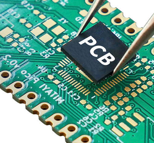
01 Design board acceptanceFactory Engineering accepts and checks the design board files sent by the customer.Checks include: design files are appropriate, layer...

Although it is easier to control when soldering on a circuit board with a large layout size, if the size of the circuit board is too large, the printed lines wi...

The scientific name for PCB is polychlorinated biphenyls. Polychlorinated biphenyls are carcinogens that easily accumulate in adipose tissue, causing diseases o...

a) The device footprint library requires the use of the wave pad library.b) The axial direction of the SOP device should be consistent with the direction of the...