
Service Hotline
Service Hotline

Time:2023-04-19 Visit:
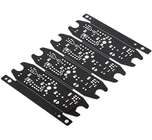
Pole (VIA) is one of the important parts of multi -layer PCB, and the cost of drilling usually accounts for 30%to 40%of the cost of PCB board. Simply put, every hole on the PCB can be called over -holes. From the perspective of action, the perforated can be divided into two categories: one is used as electrical connections between layers; the other is to be used as a fixed or positioning of the device. From the perspective of processes, holes are generally divided into three categories, namely Blind Via, Buried Via, and Through Via.
The blind hole is located on the top and bottom surface of the printing line board. It has a certain depth and is used for the connection between the surface line and the inner line below. The depth of the hole usually does not exceed a certain ratio (pore diameter). Burning holes refer to the connection holes located in the inner layer of the printing line board, which will not extend to the surface of the circuit board. The above two types of holes are located in the inner layer of the circuit board. Before the layer pressure, the through -hole molding process is completed. In the process of perforation, several inner layers may be overlapped. The third type is called Tongkou. This kind of holes pass through the entire line board and can be used to achieve internal interconnection or as component installation positioning holes. Because Tongkou is more easy to achieve in technology and low cost, most of the printing circuit boards are used, without the other two types of perforated. If there is no special explanation mentioned below, all of the excessive holes are considered as a hole.
First, from the perspective of design, a perforated is mainly composed of two parts. One is the drilling of the middle (Drill Hole), and the other is the pad pile area around the drill. The size of these two parts determines the size of the holes. Obviously, when the high -speed and high -density PCB design, the designer always wants the smaller the hole, so that there can be more wiring space on the board. In addition, the smaller the holes The smaller, the more suitable for high -speed circuits. However, the decrease in hole size has brought about increased costs, and the size of the perforated cannot be reduced without limit. The longer the hole takes, the easier it is to deviate from the center position; and when the depth of the hole exceeds 6 times the diameter of the drilling hole, it is impossible to ensure that the hole wall can be placed evenly. For example, the thickness of the 6 -layer PCB plate (through the hole depth) of the normal 6 -layer PCB now is about 50mil, so the diameter diameter that PCB manufacturers can provide can only reach 8mil.
Second, the parasitic capacitance of the perforated has a parasitic capacitor to the ground. The plate-based dielectric constant is ε, the size of the parasitic capacitance of the perforated is similar to: C = 1.41 εTdd1/(D2-D1) Paramountable parasitic capacitance will cause the circuit to extend the increase time of the signal and reduce the time of the signal and reduce The speed of the circuit. For example, for a PCB board with a thickness of 50mil, if the inner diameter is 10mil, the pile diameter is 20mil, and the distance between the pad and the copper area of the floor is 32mil, then we can use the above formula to calculate the perforated excessive excessive holes. The parasitic capacitance is roughly: C = 1.41x4.4X0.050X0.020/(0.032-0.020) = 0.517pf, the increased volume caused by this part of the capacitor is: T10-90 = 2.2C (z0/2) = 2.2 = 2.2 x0.517x (55/2) = 31.28ps. From these values, it can be seen that although the effect of rising and delay caused by a single excess parasitic capacitor is not obvious, if the excessive perforated in the wiring is used to switch between layers, the designer should consider it carefully.
Third, the parasitic inductance of the perforated is also the same. There is a parasitic capacitor with parasitic capacitors at the same time. At the same time, the parasitic inductance is also existed. In the design of high -speed digital circuits, the harm of parasitic inductors of perforated is often greater than the impact of parasitic capacitors. Its parasitic series of inductors will weaken the contribution of bypass capacitors and weaken the filter effectiveness of the entire power system. We can use the following formula to simply calculate a parasitic inductance that is approximately perforated: l = 5.08h [ln (4h/d) +1] where L refers to the inductance of the perfunction, H is the length of the perfunction, D is the center of the center, D is the center Diamond diameter. It can be seen from the formula that the influence of the diameter of the perforated diameter has less impact on the inductance, and the most impact on the inductance is the length of the perfunction. The above example still uses the above example. The inductance of the perforated is: l = 5.08x0.050 [ln (4x0.050/0.010) +1] = 1.015NH. If the signal is 1NS, the equivalent impedance size is: xl = πl/T10-90 = 3.19Ω. Such impedances can no longer be ignored in the passing of high -frequency current. In particular, it is necessary to note that bypass capacitors need to pass two perforated when connecting the power layer and the formation, so that the parasitic inductance of the perforated is doubled.

Offer competitive price with
superior quality

The indepent PCB and SMT
plant

Guarantee the quality and
lead time

Fastest processing in each
department
24H service hotline:
 sales@hyymcpcb.com
mkt@hyymcpcb.com
 No.10 YuMin Road, Shatou Industrial Zone, ShajingTown, Bao'an District, Shenzhen, China.


Copyright © 2013-2017 SHENZHEN HYY TECHNOLOGY CO.,LTD Technical Support: Xhyos


About Us

News

