Time:2022-11-02 Visit:
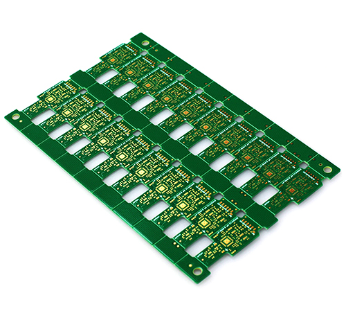
Pcb multilayer circuit board is a special kind of printed circuit board, and its "location" is generally special, for example, there will be pcb multilayer boards in the circuit board. This kind of multilayer board can help the machine to conduct various circuits, not only that, but also can play an insulating role, so that electricity will not collide with each other, and it is absolutely safe. If you want to use a PCB multilayer board with good performance, you must carefully design it. Next, we will explain how to design a PCB multilayer board.

1、 Determination of circuit board shape, size and number of layers
1. The number of layers must be determined according to the requirements of circuit performance, board size and circuit density. For multilayer printed boards, four layer boards and six layer boards are the most widely used. For example, four layer boards are two wire layers (component surface and welding surface), one power layer and one layer.
2. Each layer of PCB multilayer circuit board shall be symmetrical, and it is better to have even copper layers, namely four layer circuit board, six layer PCB, eight layer circuit board, etc. Because of the asymmetric lamination, the PCB board surface is prone to warp, especially for the surface mounted PCB multilayer circuit board, which should be paid more attention.
3. Any printed circuit board has the problem of matching with other structural parts. Therefore, the shape and size of the printed circuit board must be based on the overall structure of the product. However, from the perspective of production technology, it should be as simple as possible. Generally, it is a rectangle with a small ratio of length to width, which is conducive to improving production efficiency and reducing labor costs.
2、 Position and placement direction of components
1. On the other hand, the overall structure of the printed circuit board should be considered to avoid uneven arrangement of components. This not only affects the aesthetics of printed boards, but also brings a lot of inconvenience to assembly and maintenance.
2. The location and placement direction of components should first be considered from the circuit principle to meet the trend of the circuit. Whether the placement is reasonable or not will directly affect the performance of the printed circuit board, especially the high-frequency analog circuit, which has more stringent requirements on the location and placement of devices.
3. The reasonable placement of components, in a sense, has indicated the success of the PCB design. Therefore, when preparing the layout of printed boards and deciding the overall layout, the circuit principle should be analyzed in detail, and the location of special components (such as large-scale IC, high-power tubes, signal sources, etc.) should be determined first, and then other components should be arranged to avoid possible interference factors.