Time:2022-08-15 Visit:
But when it comes to the layout of artistic components in PCB planning, the problem becomes interesting.

1. Clarify board physical constraints
Before placing components, you first need to know exactly the mounting holes of the circuit board, the position of the edge connectors, and the mechanical size constraints of the circuit board. why?
Because these factors affect the size and shape of your board. I have seen a certain designed circuit board not fit into the fixed area of the circuit board, so I had to design it from scratch.
In order to prevent foolishness, you can intentionally set a clear area for those mechanical constraints (device holes, circuit outlines), so that you can focus on creating within the allowed range.
2. Clarify the circuit board manufacturing process
Likewise, before placing circuit components, you'd better clarify a few key pieces of information from the circuit manufacturer:
Circuit assembly process and test process;
Whether it is necessary to reserve space for PCB V-grooving;
Element equipment welding process: is it wave soldering, zoned soldering or manual soldering?
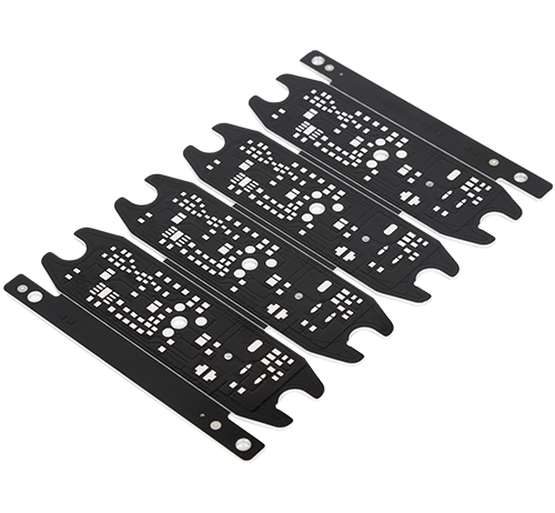
The circuit board manufacturing process will affect the size of the space between components. Also, if your board will be soldered on the assembly line in the future, you will need to leave a nominal space (greater than 20mil) on the edge of the board for the board to be attached to the conveyor belt. The rated mounting plate on the circuit board, which is broken off after the circuit board is soldered.