
Service Hotline
Service Hotline

Time:2023-04-11 Visit:
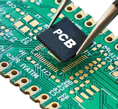
When designing PCB pads in PCB board design, it is necessary to design strictly in accordance with the relevant requirements standards. Because in SMT patch processing, the design of PCB pads is very important. The design of pads will directly affect the welding, stability and thermal energy transmission of the components. what?
1. The design standards of the shape and size of PCB pads:
1. Call the PCB standard packaging library.
2. The minimum unilateral unilateral pad is not less than 0.25mm.
3. Try to ensure that the distance between the edges of the two pads is greater than 0.4mm.
4. Pore diameter exceeding 1.2mm or pads with a diameter of more than 3.0mm should be designed as diamond -shaped or plum -shaped pads
5. When the wiring is dense, it is recommended to use oval and long circular connectors. The diameter or minimum width of the single -to -panel pad is 1.6mm; the weak electric line pads of the double panel can only be added with 0.5mm in diameter, and the pads are too large to cause unnecessary welding.
Second, PCB pads pass through hole size standards:
The inner holes of the pads are generally not less than 0.6mm, because the pores that are less than 0.6mm are not easy to process when punching the punching. Generally, the diameter value of the metal pin plus 0.2mm is used as the diameter of the pile. When it is 0.5mm, the diameter of the pad pads corresponds to 0.7mm, and the diameter of the pad depends on the diameter of the inner hole.
Third, the main points of the reliability design of PCB pads:
1. Symmetry, in order to ensure the balance of the surface tension of the melting welding, the pads of both ends must be symmetrical.
2. The spacing of the pad, too large or too small the pads can cause welding defects. Therefore, the spacing of the component end or pin and the pad is appropriate.
3. The remaining size of the pads, the remaining size of the component end or pins and pads must ensure that the welding joint can form a curved moon surface.
4. The width of the pads should be basically the same as the width of the end or pins of the component.
The correct PCB pad design. If there is a small amount of skew during the processing of the patch, it can be corrected due to the effect of the surface tension of the melting weld during re -welding. And if the PCB pad design is incorrect, even if the installation location is very accurate, the component position bias and suspension bridge will occur after the streaming position is very accurate. Therefore, the PCB pad design needs to be paid great attention to the PCB pad design.

Offer competitive price with
superior quality

The indepent PCB and SMT
plant

Guarantee the quality and
lead time

Fastest processing in each
department
24H service hotline:
 sales@hyymcpcb.com
mkt@hyymcpcb.com
 Block B, NO.8 Minfu Road, Shatou Industrial Park, Shajing Town, Bao'an District, Shenzhen, Guangdong, China, 518000


Copyright © 2013-2017 SHENZHEN HYY TECHNOLOGY CO.,LTD Technical Support: Nbone


About Us

News

