
Service Hotline
Service Hotline

Time:2023-03-21 Visit:
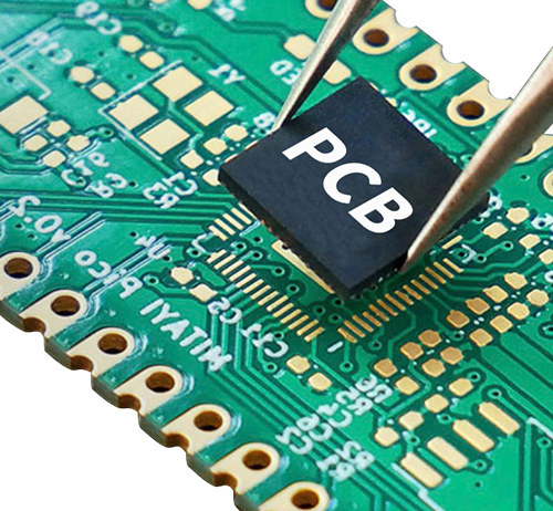
In the process of PCB design, if possible in advance to predict possible risks and avoid them in advance, the success rate of PCB design will be greatly improved. Many companies have an indicator of the success rate of PCB design when they evaluate projects.
The key to improving the success rate of one board lies in the design of signal integrity. At present, there are many product solutions, and chip manufacturers have been done, including what chips are used, how to build peripheral circuits, and so on. Hardware engineers often do not need to consider the problem of circuit principles, just need to make the PCB by themselves.
But in the process of PCB design, many companies have encountered difficulties, either unstable in designing PCB or not working. For large enterprises, many chip manufacturers will provide technical support to guide PCB design. But some small and medium -sized enterprises are difficult to get this support. Therefore, you must find a way to complete it yourself, so there are many problems. You may need to play several versions and debug for a long time. In fact, if you understand the design method of the system, these can be avoided. Next, let's talk about the three techniques to reduce the risk of PCB design.
1. The system planning stage is best to consider the problem of signal integrity. Can the entire system be built like this, can the signal be transmitted from one PCB to another PCB to receive it correctly? This is necessary to evaluate in the early stage, and it is not difficult to evaluate this problem. Knowing a little signal integrity knowledge, a simple software operation can be done.
2. In the process of PCB design, use the simulation software to evaluate the specific wiring to observe whether the quality of the signal can meet the requirements. This simulation process itself is very simple. The key is to understand the principles of signal integrity and be used to guide.
3. In the process of doing PCB, risk control must be performed. There are many problems. At present, the simulation software has no way to solve it, and the designer must be manually controlled. The key to this step is to understand where there will be risks and how to do to avoid risks. What is needed is the signal integrity knowledge.

Offer competitive price with
superior quality

The indepent PCB and SMT
plant

Guarantee the quality and
lead time

Fastest processing in each
department
24H service hotline:
 sales@hyymcpcb.com
mkt@hyymcpcb.com
 Block B, NO.8 Minfu Road, Shatou Industrial Park, Shajing Town, Bao'an District, Shenzhen, Guangdong, China, 518000


Copyright © 2013-2017 SHENZHEN HYY TECHNOLOGY CO.,LTD Technical Support: Nbone


About Us

News

