
Service Hotline
Service Hotline

Time:2023-03-03 Visit:
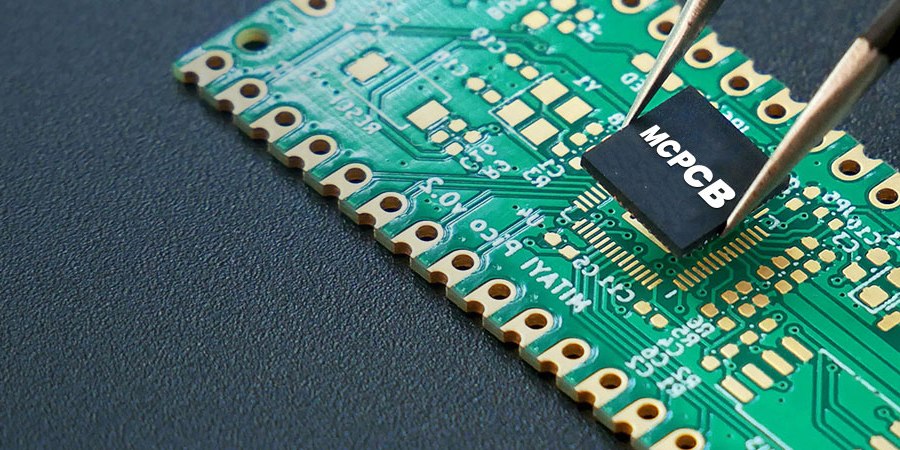
1. The weldability of the circuit plate hole affects the quality of welding
The circuit plate holes are not welded well, which will cause virtual welding defects, affect the parameters of the components in the circuit, cause the multi -layer board component and the inner line to be unstable, and cause the entire circuit function to fail. The so -called weldability is the properties of the metal surface being wet welded, that is, the surface of the metal where the solder is located forms a relatively uniform and continuous and smooth attachment film. Factors affecting the weldability of the printing circuit board are: (1) the ingredients of the solder and the properties of the welded. Welded is an important part of the welding chemical treatment process. It consists of chemical materials containing helping welds. The commonly used low-melting point co-melting metal is SN-PB or SN-PB-AG. , To prevent welded welds from being produced by impurities. The function of the solder is to help the welded wetting of the welded circuit surface by transmitting the heat to remove the rust. Generally, white pine and isopropanol solvents are used. (2) Welding temperature and surface cleaning of metal plates will also affect weldability. If the temperature is too high, the weld diffusion speed is accelerated. At this time, it has high activity, which will quickly oxidize the circuit board and welded surface, which will cause welding defects. The pollution of the circuit board surface will also affect the weldability and cause defects. These defects will be defective. These defects will be defective. These defects will Including tin Zhuzhu, tin balls, open roads, not good gloss, etc.
2. Welding defects caused by warranty
Circuit boards and components are warped during welding, which causes deficiency such as virtual welding and short circuit due to stress deformation. Treasures are often caused by unbalanced temperatures of the upper and lower part of the circuit board. The large PCB board will also be warped due to the weight of the board. Ordinary PBGA devices are about 0.5mm from the printing circuit board. If the device on the circuit board is large, as the circuit board recesses the normal shape, the solder joint will be under stressing for a long time. Virtual welding road.
3. The design of the circuit board affects the welding quality
In terms of layout, when the size of the circuit board is too large, although the welding is easier to control, the printing lines are long, the impedance increases, the anti -noise ability decreases, and the cost increases. Interference, such as electromagnetic interference of the circuit board. Therefore, the PCB board design must be optimized: (1) shorten the connection between high -frequency components and reduce EMI interference. (2) The weight (such as more than 20g) components shall be fixed with a bracket and then welded. (3) The heat dissipation problem should be considered to prevent the surface of the component from large Δt to produce defects and rework. Thermal components should be away from the heating source. (4) The arrangement of components is as parallel as possible. This is not only beautiful but also easy to weld, and large quantities should be performed. The circuit board is designed with a rectangle of 4: 3. Do not change the width of the wire to avoid the discontinuousness of the wiring. When the PCB board is heated for a long time, copper foil is prone to expand and fall off. Therefore, a large area of copper foil should be avoided.

Offer competitive price with
superior quality

The indepent PCB and SMT
plant

Guarantee the quality and
lead time

Fastest processing in each
department
24H service hotline:
 sales@hyymcpcb.com
mkt@hyymcpcb.com
 Block B, NO.8 Minfu Road, Shatou Industrial Park, Shajing Town, Bao'an District, Shenzhen, Guangdong, China, 518000


Copyright © 2013-2017 SHENZHEN HYY TECHNOLOGY CO.,LTD Technical Support: Nbone


About Us

News

