
Service Hotline
Service Hotline

Time:2022-12-19 Visit:
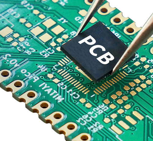
1. Get a PCB, and first record the models, parameters, and positions of all components on the paper, especially the directions of diodes, transistors, and IC notches. It is better to take two photos of component positions with a digital camera. The current PCB is becoming more and more advanced, and the diode triode on it is not noticeable.
2. Remove all high precision PCB multilayer boards and remove the tin in the PAD hole. Clean the PCB with alcohol, and then put it into the scanner. When the scanner scans, it needs to slightly increase the scanning pixels to get a clearer image. Then polish the top layer and bottom layer slightly with water gauze until the copper film is bright, put it into the scanner, start PHOTOSHOP, and sweep the two layers in color. Note that the PCB must be placed horizontally and vertically in the scanner, otherwise the scanned image cannot be used.
3. Adjust the contrast and lightness of the canvas to make the part with copper film contrast strongly with the part without copper film, and then turn the secondary image to black and white to check whether the lines are clear. If not, repeat this step. If the image is clear, save it as a black and white BMP file TOP.BMP and BOT.BMP. If you find a problem with the image, you can also use PHOTOSHOP to repair it.
4. Convert two BMP files into PROTEL files, and call in two layers in PROTEL. If the positions of PAD and VIA passing through two layers basically coincide, it indicates that the previous steps are well done. If there is any deviation, repeat the third step. Therefore, PCB copying is a very patient work, because a small problem will affect the quality and the matching degree after copying.
5. Convert BMP of TOP layer to TOP PCB, pay attention to convert to SILK layer, which is the yellow layer. Then you can trace lines on TOP layer, and place devices according to the drawing in step 2. Delete SILK layer after drawing. Repeat until all layers are drawn.

Offer competitive price with
superior quality

The indepent PCB and SMT
plant

Guarantee the quality and
lead time

Fastest processing in each
department
24H service hotline:
 sales@hyymcpcb.com
mkt@hyymcpcb.com
 Block B, NO.8 Minfu Road, Shatou Industrial Park, Shajing Town, Bao'an District, Shenzhen, Guangdong, China, 518000


Copyright © 2013-2017 SHENZHEN HYY TECHNOLOGY CO.,LTD Technical Support: Nbone


About Us

News

